Source Code: iamJohnnySam/AlignerSimulator: Semiconductor Aligner Sensor Simulator
Visualizing the Raw Sensor Data Behind Wafer Alignment
Modern semiconductor equipment relies heavily on precision alignment. Before any lithography, inspection, or processing step can happen, the wafer must be perfectly centered and oriented.
One of the most important subsystems responsible for this is the wafer aligner.
To help students, engineers, and algorithm developers understand how aligners actually “see” a wafer, I built a Wafer Aligner Simulator that generates realistic line-sensor data for wafers from 100 mm to 450 mm as well as SEMI G74 tape frames.
This article explains how wafer alignment works and how this simulator can help you explore the physics and mathematics behind it.
Why Wafer Alignment Matters
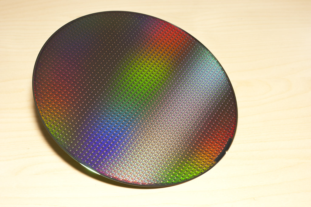
A silicon wafer may look perfectly circular, but in reality it contains orientation features that indicate crystal direction and allow machines to orient the wafer consistently.
These include:
- Notches (modern wafers)
- Primary and secondary flats (older wafers)
- Alignment notches on tape frames
If a wafer is even slightly misaligned, the entire process chain can fail:
- Lithography overlays become inaccurate
- Die placement shifts
- Pick-and-place tools mis-handle wafers
- Yield drops dramatically
Alignment accuracy requirements are typically in the tens of microns.
How a Wafer Aligner Actually Works
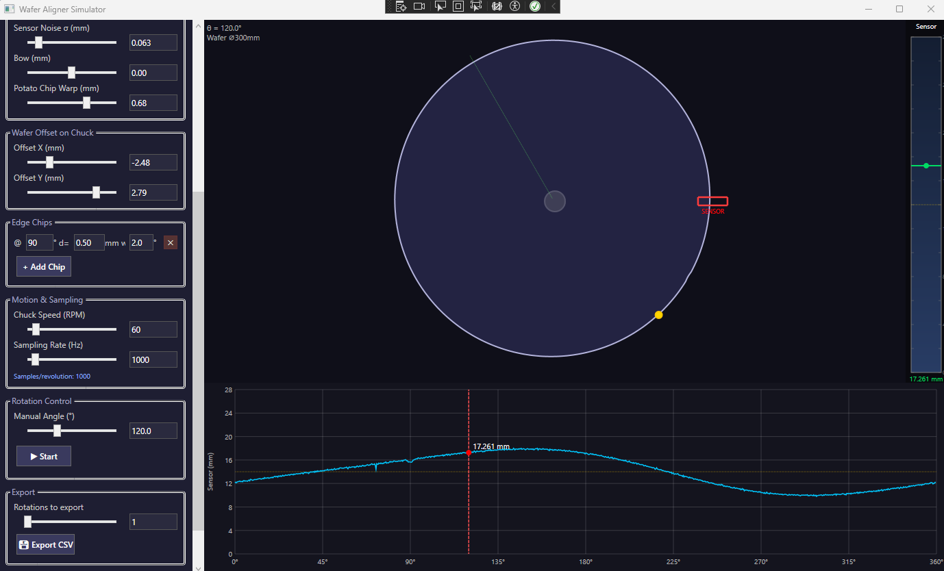
Most aligners use a fixed optical edge sensor while the wafer rotates on a chuck.
Instead of “seeing” the wafer as an image, the sensor measures distance to the wafer edge along a single radial line.
As the wafer rotates, the sensor produces a waveform like this:

This waveform should contain everything needed to determine:
- Wafer center offset
- Notch/flat position
- Wafer orientation angle
- Edge defects and chips
The Measurement Geometry
The geometry is simple but powerful:
- Wafer sits on a rotating chuck
- A fixed sensor looks toward the center
- As the wafer rotates, the sensor measures the edge radius
Mathematically:
SensorReading = intersection(sensor_line, wafer_edge(angle))If the wafer were perfect and centered, the sensor would output a constant value.
But real wafers are never perfect.
What Real Sensors Actually See
Real aligner signals contain many effects:
- Notch / Flat: Large dip in radius
- Center offset: Sinusoidal variation
- Bow / warp: Low-frequency drift
- Edge chips: Sharp local spikes
- Sensor noise: Random jitter
Understanding how these effects combine is critical for designing robust alignment algorithms.
Why I Built This Simulator
Access to real aligner hardware is limited.
Students and junior engineers rarely get exposure to raw sensor data.
So I built a real-time simulator that recreates what an optical edge sensor would output.
The simulator models:
Supported Substrates
- 50–450 mm wafers
- Notch wafers
- Single & double flat wafers
- SEMI G74 tape frames
Realistic Imperfections
- Bow and warp (potato chip effect)
- Centering errors
- Edge chips and damage
- Sensor noise
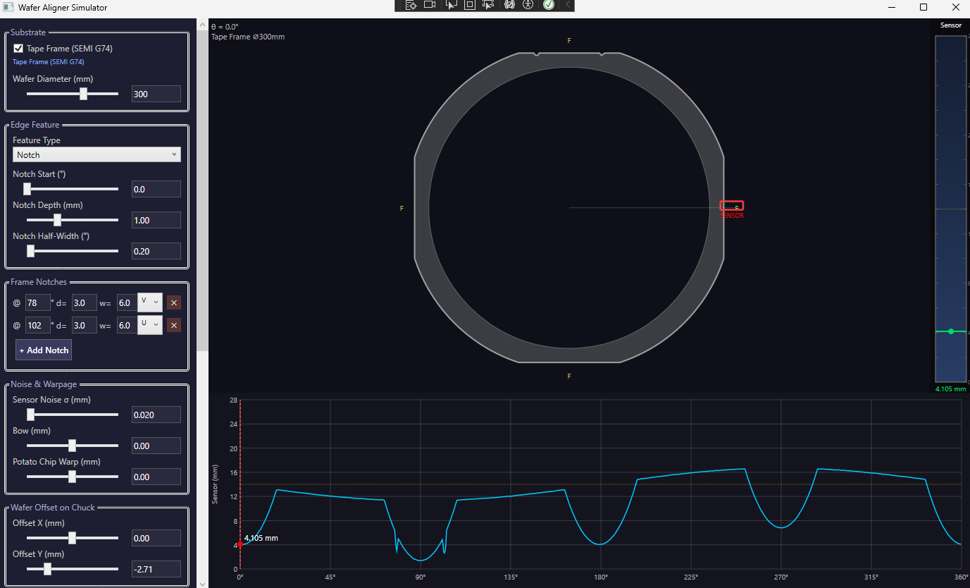
Real-Time Visualization
The application shows three synchronized views:
- Top-down wafer view
- Sensor value bar (0–28 mm range)
- Angle vs sensor reading chart
This lets users see geometry and signal simultaneously.
From Geometry to Signal: The Key Idea
At each angle θ, the simulator computes the wafer radius:
r(θ) = BaseGeometry
+ Notch/Flats
+ Bow/Warp
+ Edge Chips
+ Center Offset
+ Noise
The final sensor waveform is generated by simulating ray intersection with the wafer edge.
This allows users to test alignment algorithms using physically realistic datasets.
Tape Frame Alignment (SEMI G74)
One unique capability of the simulator is support for tape frame substrates.
Tape frames are not circular — they are a rounded square profile with multiple alignment notches.
This creates a very different sensor waveform and presents interesting algorithm challenges.
Exporting Realistic Sensor Data
The simulator can export high-resolution CSV datasets:
SampleIndex, TimeMs, AngleDeg, SensorValueMmThis enables:
- MATLAB / Python analysis
- Machine learning dataset generation
- Algorithm benchmarking
- Regression testing
Students can go from visual understanding → real data → algorithm design.
Educational Value
This project is especially useful for:
Students
- Understand wafer alignment fundamentals
- Learn geometric measurement techniques
- Visualize real sensor behavior
Engineers
- Prototype alignment algorithms
- Test edge cases before hardware exists
- Generate training datasets
Equipment Developers
- Validate sensor specs
- Study tolerance sensitivity
- Explore failure scenarios
Example Learning Exercises
Students can experiment with questions like:
- How does wafer offset appear in the signal?
- How do chips cause false notch detection?
- How does chuck speed affect sampling requirements?
- Can you detect flats with heavy noise?
This makes wafer alignment interactive and intuitive.
Future Plans
Potential improvements include:
- Multi-sensor aligner configurations
- 3D wafer topology modeling
- Importing real hardware data
- Advanced noise models
- Automated test-case generation
Conclusion
Wafer alignment is one of the most fundamental — yet least visible — steps in semiconductor manufacturing.
By simulating the raw sensor data behind alignment, this project helps bridge the gap between theory, algorithms, and real equipment.
If you're teaching semiconductor engineering, developing aligner algorithms, or just curious how wafer alignment works, this simulator provides a powerful way to explore the system from first principles.