Semiconductor Basics
- Semiconductor Manufacturing | Electrical Engineering and Computer Science | MIT OpenCourseWare
- Types of Semiconductor Devices | Toshiba Electronic Devices & Storage Corporation | Americas – United States (semicon-storage.com)
- Semiconductor Technology (Online Version) | Semitracks
Basic Fab breakdown
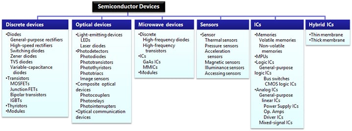
- Digital IC
- Logic (data processing)
- Memory (data storage)
- Analog IC
- Mixed Signal IC
The MOSFET
Metal Oxide Semiconductor Field Effect Transistor. These are the basic building blocks of our chips.
What is High-k? Definition of High-K/Metal Gate | PCMag
Before FinFET teachnology, when the length of the gate electrode was required to be reduced the control of the gate over the channel region was also reduced. As a solution High-k Metal Gate (HKMG) enabled to continue this reduction by reducing the leakage more than 100x compared to standard Silicon Oxide gate. Due to the high-k, the Drive current is enhanced.

Combining MOSFET for Logical Operations
Used for controlling flow of data and operations within systems such as Logic or Arithmatic operations. These chips are found in CPU's, GPU's or Microcontrollers.
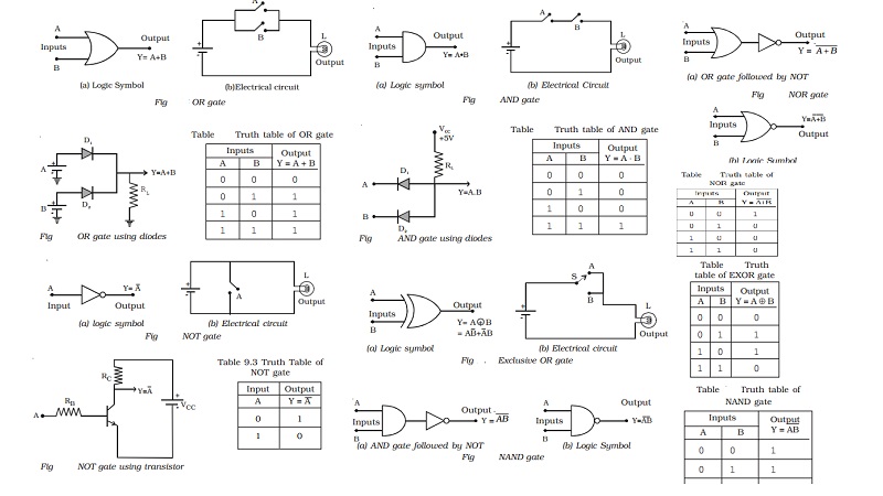
Logic functions are represented in theory using Logic Gates. Gates can be interconnected together to perform very complex computations.

Processors also come with Static Random Access Memory (SRAM) to hold data and instructions being used by the processor. Below is an image of a 6-transistor SRAM and how it would be fabricated in the real world.
![]()

For more information please check - imec magazine September 2017 - The vertical nanowire FET: enabler of highly dense SRAMs (imec-int.com)
Inside the chip there are a lot of interconnects that connect together many transistors or circuits made up of transistors. If the transistors are made up on the lowest layers, there will be many layers on top for interconnecting all transistors to make 1 large and complex circuit to perform some operation.

Manufacturing Features
Shallow Trench Isolation
- Box isolation technique
- Used to electrically isolate regions
- Regularly used on CMOS process technology nodes of < 250nm

Manufactruring Methods
Manufactruring Process
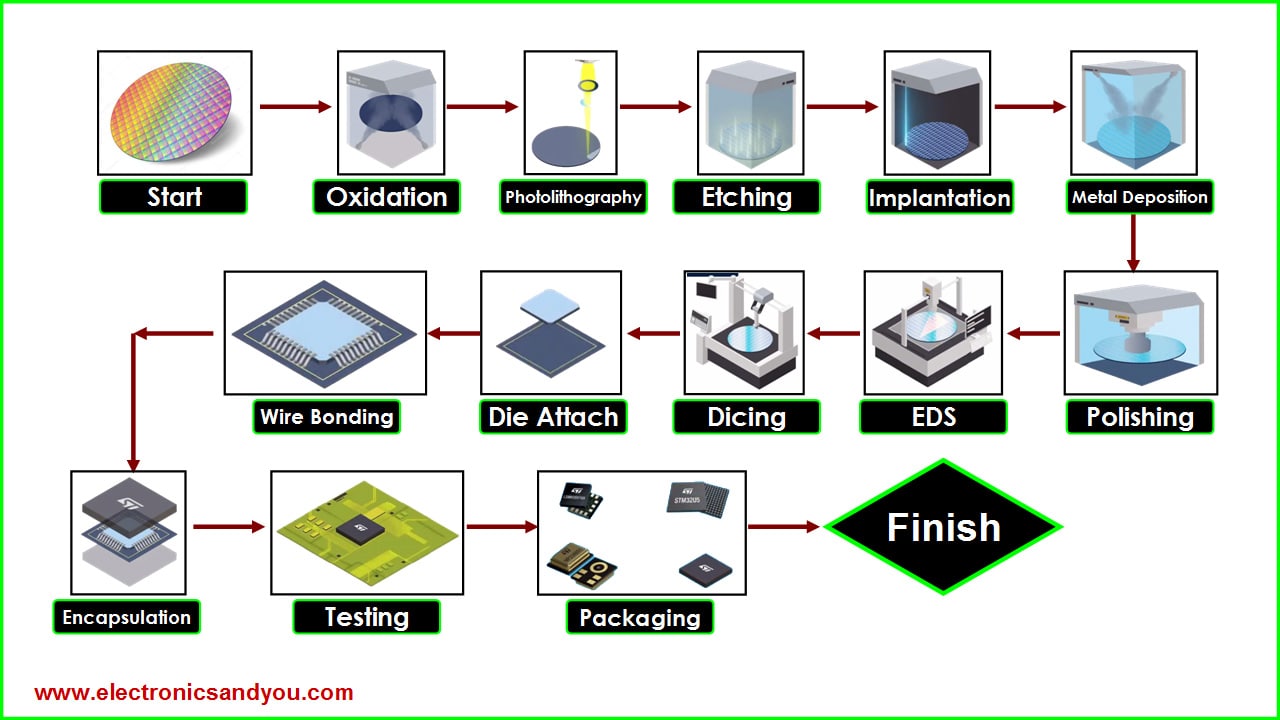
- Wafer Manufacturing
- Oxidation
- Photolithography
- Etching
- Deposition & ion implementation
- Metal wiring
- EDS
- Packaging
Wafer Manufacturing
Photolithography
Wafer Sawing
Wire Bonding
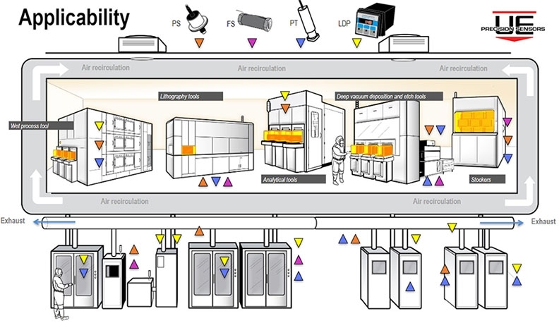
Inside a Fab
References
- Understanding the Semiconductor Industry – Apex Waves | Blog
- Types of Semiconductor Devices | Toshiba Electronic Devices & Storage Corporation | Americas – United States (semicon-storage.com)
- The Role of the Logic Gate | demystifying digital electronics – Computer Engineering for Babies
- Basic logic gates using discrete components (brainkart.com)
- imec magazine September 2017 - The vertical nanowire FET: enabler of highly dense SRAMs (imec-int.com)
- ã€ç¦ç”°æ˜ã®ã‚»ãƒŸã‚³ãƒ³æ¥ç•Œæœ€å‰ç·šã€‘12月開催ã®IEDM 2017ã§æŠ«éœ²ã•ã‚Œã‚‹æ¬¡ä¸–代ã®åŠå°Žä½“è£½é€ æŠ€è¡“ã¨ãƒ¡ãƒ¢ãƒªæŠ€è¡“ - PC Watch (impress.co.jp)
- Intel Technology - YouTube
- Definition of High-K/Metal Gate | PCMag
- Shallow trench isolation - Wikipedia
- Semiconductor Manufacturing Process Products and Applicability | Valin