Getting Started
There is a lot of information that is needed to get started. Here I have listed some videos that helped me when I got started.

If you are interested to learn more, please have a look at these links which includes some factory tours and different explanations on the semiconductor manufacturing process.
- https://youtu.be/c9arR8T0Qts
- https://youtu.be/bor0qLifjz4
- https://youtu.be/EFGom2z4mlQ
- https://youtu.be/6OeYwfDkiH8
- https://youtu.be/d9SWNLZvA8g
- https://youtu.be/7DlNIhuuPvM
- https://youtu.be/LjDUROWxT7k
- Bosch chip factory Dresden | Bosch Global
- SemiWiki - All Things Semiconductor!
The playlist of 15 videos below provides some deep dive in to each aspect of Semiconductor manufacturing.
Who are the Big Players in this industry
- ASM
- ASM supplies wafer processing equipment to the leading semiconductor manufacturers, mostly for the deposition of thin films. They design, manufacture, sell, and service deposition tools to supply our customers with the advanced technologies to produce semiconductor devices, or integrated circuits (ICs).
- Mattson Technology, Inc.
-
Mattson Technology, Inc. designs, manufactures, markets and globally supports semiconductor wafer processing equipment used in the fabrication of integrated circuits. They are a key supplier of plasma and rapid thermal processing equipment to the global semiconductor industry. Their processing equipment utilizes innovative technologies to deliver advanced processing capabilities and high productivity for the fabrication of current and next-generation integrated circuits. Our equipment and technologies are used by leading memory, foundry and logic device manufacturers, worldwide. New innovations from Mattson Technology in Atomic Surface Engineering TM address the most critical 3D logic and memory manufacturing challenges
-
- K&S
- Kulicke and Soffa Industries, Inc. specialize in developing cutting-edge semiconductor and electronics assembly solutions enabling a smarter and more sustainable future. Their ever-growing range of products and services supports growth and facilitates technology transitions across large-scale markets, such as advanced display, automotive, communications, compute, consumer, data storage, energy storage and industrial.
- MindoxTechno
- Jabil
Industry Standards
Majority of the semiconductor industry is governed by SEMI standards (Shop semi.org).
Some of the commonly referred SEMI standards for equipment manufacturing would be as follows.
- E Series: Equipment Communications
- E00109 - SEMI E1.9 - Mechanical Specification for Cassettes Used to Tr
- E01500 - SEMI E15 - Specification for Tool Load Port
- E01501 - SEMI E15.1 - Specification for 300 mm Tool Load Port
- E04701 - SEMI E47.1 - Mechanical Specification for FOUPS Used to Transport anf Store 300mm Wafers
- E06200 - SEMI E62 - Specification for 300 mm Front-Opening Interface Mechanical Standard (FIMS)
- E07200 - SEMI E72 - Specification and Guide for Equipment Footprint, H
- SEMI E78 - Guide to Assess and Control Electrostatic Discharge (ESD) and Electrostatic Attraction (ESA) for Equipment
- E08400 - SEMI E84 - Specification for Enhanced Carrier Handoff Paralle
- E08700 - SEMI E87 - Specification for Carrier Management (CMS)
- E11900 - SEMI E119 - Mechanical Specification for Reduced-Pitch Front-
- E15300 - SEMI E153 - Specification for AMHS SEM (AMHS SEM)
- E18400 - SEMI E184 - Specification for 300 mm Tape Frame FOUP Load Port
- E18500 - SEMI E185 - Specification for 300 mm Tape Frame FOUP
- G Series: Packaging
- S Series: Safety, Environmental and Energy
- S00100 - SEMI S1 - Safety Guideline for Equipment Safety Labels
- S00200 - SEMI S2 - Environmental, Health, and Safety Guideline for Semiconductor Manufacturing Equipment
- S00600 - SEMI S6 - Environmental, Health, and Safety Guideline for Exhaust Ventilation of Semiconductor Manufacturing Equipment
- S00800 - SEMI S8 - Safety Guideline for Ergonomics Engineering of Semiconductor Manufacturing Equipment
- S01000 - SEMI S10 - Safety Guideline for Risk Assessment and Risk Evaluation Process
- S02200 - SEMI S22 - Safety Guideline for the Electrical Design of Semiconductor Manufacturing Equipment
UL is also a widely recognized standard specially for Electrical components which are govered by UL508A
SECS/GEM
Overview of GEM Standard Video Part 1 (cimetrix.com)

SECS Message Code Generation Tool (hume.com)

Substrates and their sizes
Primarily the substrate processed will be the wafer. However, the wafer can be receieved as a bare wafer on fitted on to a frame with a film or tape (called tape frame or film frame) for purposes of handling during dicing.
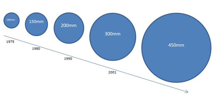
When it comes to silicon wafers, there are 3 major sizes of wafers currently being used in industry as of 2023.
- 150mm (5.9 inch - reffered to as 6 inch)
- 200mm (7.9 inch - reffered to as 8 inch)
- 300mm (11.8 inch - reffered to as 12 inch)
The next thing to keep in mind about silicon wafers is that they come with either a notch or a flat side for the purposes of orienting the wafer.
- Under 200mm diameter = flat
- Over 200mm diameter = notch
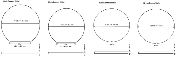
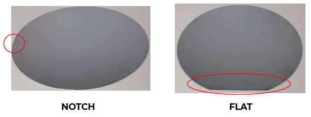
For wafers which have a flat side, based on different surface treatment, but this is not always used.

In terms of tape frame / film frame there are a few standard sizes based on the wafer size which can be seen below
Some Abriviations used in the industry
Having worked in a number of industries before, one of the most disorienting things at the start of your career can be all the abbriviations that get thrown around and everyone in the room uses them like they are standard words in the English vocabulary. These are some of the common abbrivations that I have come across.
|
AMC |
Airborne Molecular Contamination |
|
API |
Application Program Interface |
|
APR |
Automatic Pressure Regulator |
|
AWH |
Auto Wafer Hander |
|
BLDC |
Brushless DC |
|
BTP |
Built to Print |
|
C2W |
Chip to Wafer |
|
CDA |
Compressed Dry Air |
|
CIM |
Computer-Integrated Manufacturing |
|
CM |
Control Module |
|
CR |
Carriage Return |
|
EE |
End Effector |
|
EFEM |
Equipment Front End Module |
|
EMO |
Emergency Machine Off |
|
EtherCAT |
Ethernet for Control Automation Technology |
|
FAT |
Factory Acceptance Test |
|
FFU |
Fan Filter Unit |
|
FI |
Factory Interface (EFEM) |
|
FOA |
Fab Owners Alliance |
|
FOSB |
Front Opening Shipping Box |
|
GEM |
Generic Equipment Model |
|
GUI |
Graphical User Interface |
|
HSMS |
High-Speed SECS Message Services |
|
I/O |
Input Output |
|
ICU |
Inductive Control Unit |
|
IETF |
Internet Engineering Task Force |
|
IPC |
Industrial PC |
|
LCU |
Local Control Unit |
|
LF |
Line Feed |
|
LL |
Load Lock |
|
LOTO |
Lockout Tagout |
|
LP |
Load Port |
|
LPM |
Load Port Module |
|
LV32 |
Local Viewer 32 |
|
MES |
Manufacturing execution system |
|
MFC |
Mass Flow Controller |
|
MPDU |
Main Power Distribution Unit |
|
MPPS |
Most Penetrating Particle Size |
|
MSIG |
MEMS & Sensors Industry Group |
|
OCR |
Optical Character Recognition |
|
OEM |
Original Equipment Manufacturer |
|
OHT |
Overhead Track |
|
PCW |
Process Cooling Water |
|
PLP |
Panel Level Packaging |
|
PM |
Process Module |
|
PR |
Pressure Switch/ Pressure Regulator |
|
PT |
Pressure Switch/ Pressure Transducer |
|
PV |
Pressure Valve |
|
RFID |
Radio Frequency Identification |
|
RIM |
Remote Interface Module |
|
RPM |
Rotation Per Minute |
|
SECS |
SEMI Equipment Communications Standard |
|
SSPS |
Site & System Preparation Specification |
|
TCB |
Thermo Compression Bonding |
|
TCP |
Transmission Control Protocol |
|
UI |
User Interface |
|
ULPA |
Ultra Low Particulate Air |
|
WLP |
Wafer-level packaging |
|
WPF |
Windows Presentation Foundation |
General Practices
FFU
- Glass Fibre Filter for FFU is not allowed (PTFE is preferred)